


——Shared from DWIN Froum
Using DWIN T5L1 chip as the control core of the whole machine, receives and processes touch, ADC acquisition, PWM control information, and drives the 3.5-inch LCD screen to display the current status in real time. Support remote touch adjustment of LED light source brightness through WiFi module, and support voice alarm.
Program features:
1. Adopt T5L chip to run at high frequency, AD analog sampling is stable, and the error is small;
2. Support TYPE C directly connected to PC for debugging and program burning;
3. Support high-speed OS core interface, 16bit parallel port; UI core PWM port, AD port lead out, low-cost application design, no need to add additional MCU;
4. Support WiFi, Bluetooth remote control;
5. Support 5~12V DC wide voltage and wide range input
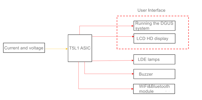
1.1 Scheme diagram
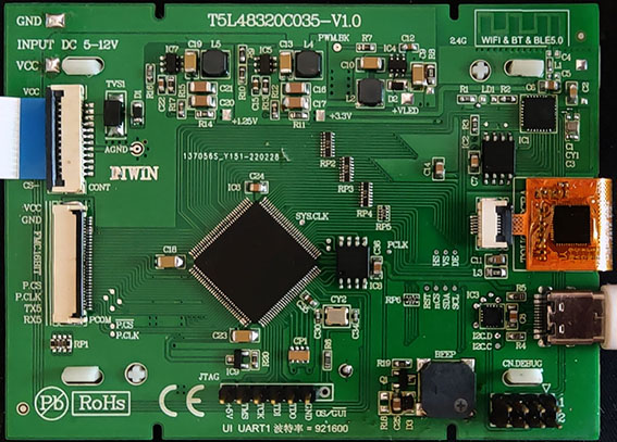
1.2 PCB board
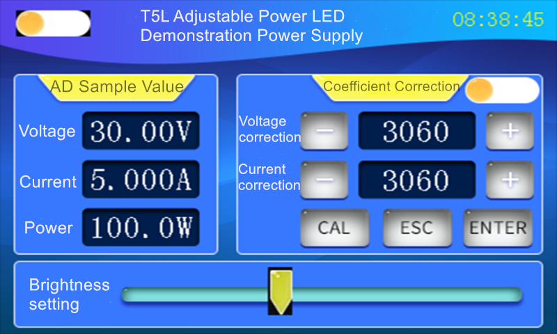
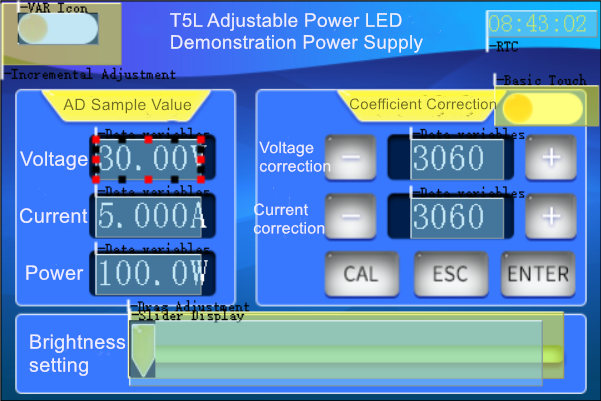
1.3 User interface
Shame introduction:
(1)Hardware circuit design
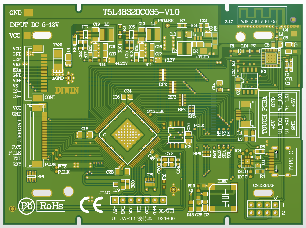
1.4 T5L48320C035 circuit diagram
1. MCU logic power supply 3.3V: C18, C26, C27, C28, C29, C31, C32, C33;
2. MCU core power supply 1.25V: C23, C24;
3. MCU analog power supply 3.3V: C35 is the analog power supply for MCU. When typesetting, the core 1.25V ground and the logic ground can be combined together, but the analog ground must be separated. The analog ground and the digital ground should be collected at the negative pole of the LDO output large capacitor, and the analog positive pole should also be collected at the positive pole of the LDO large capacitor, so that AD sampling Noise is minimized.
4. AD analog signal acquisition circuit: CP1 is the AD analog input filter capacitor. In order to reduce the sampling error, the analog ground and digital ground of the MCU are separated independently. The negative pole of CP1 must be connected to the analog ground of the MCU with minimum impedance, and the two parallel capacitors of the crystal oscillator are connected to the analog ground of the MCU.
5. Buzzer circuit: C25 is the power supply capacitor for the buzzer. The buzzer is an inductive device, and there will be a peak current during operation. In order to reduce the peak, it is necessary to reduce the MOS drive current of the buzzer to make the MOS tube work in the linear region, and design the circuit to make it work in the switch mode. Note that R18 should be connected in parallel at both ends of the buzzer to adjust the sound quality of the buzzer and make the buzzer sound crisp and pleasant.
6. WiFi circuit: WiFi chip sampling ESP32-C, with WiFi+Bluetooth+BLE. On the wiring, the RF power ground and the signal ground are separated.
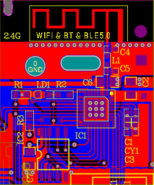
1.5 WiFi circuit design
In the above figure, the upper part of the copper coating is the power ground loop. The WiFi antenna reflection ground loop must have a large area to the power ground, and the collection point of the power ground is the negative pole of C6. A reflected current needs to be provided between the power ground and the WiFi antenna, so there must be copper coating under the WiFi antenna. The length of the copper coating exceeds the extension length of the WiFi antenna, and the extension will increase the sensitivity of the WiFi; point at the negative pole of C2. A large area of copper can shield the noise caused by the WiFi antenna radiation. The 2 copper grounds are separated on the bottom layer and collected to the middle pad of ESP32-C through vias. The RF power ground needs a lower impedance than the signal ground loop, so there are 6 vias from the power ground to the chip pad to ensure a sufficiently low impedance. The ground loop of the crystal oscillator cannot have RF power flowing through it, otherwise the crystal oscillator will generate frequency jitter, and the WiFi frequency offset will not be able to send and receive data.
7. Backlight LED power supply circuit: SOT23-6LED driver chip sampling. The DC/DC power supply to the LED independently forms a loop, and the DC/DC ground is connected to the 3.3V LOD ground. Since the PWM2 port core has been specialized, it outputs a 600K PWM signal, and an RC is added to use the PWM output as an ON/OFF control.
8. Voltage input range: two DC/DC step-downs are designed. Note that the R13 and R17 resistors in the DC/DC circuit cannot be omitted. The two DC/DC chips support up to 18V input, which is convenient for external power supply.
9. USB TYPE C debug port: TYPE C can be plugged and unplugged forwards and backwards. Forward insertion communicates with the WIFI chip ESP32-C to program the WIFI chip; reverse insertion communicates with the XR21V1410IL16 to program the T5L. TYPE C supports 5V power supply.
10. Parallel port communication: T5L OS core has many free IO ports, and 16bit parallel port communication can be designed. Combined with ST ARM FMC parallel port protocol, it supports synchronous read and write.
11. LCM RGB high-speed interface design: T5L RGB output is directly connected to LCM RGB, and buffer resistance is added in the middle to reduce LCM water ripple interference. When wiring, reduce the length of the RGB interface connection, especially the PCLK signal, and increase the RGB interface PCLK, HS, VS, DE test points; the SPI port of the screen is connected to the P2.4~P2.7 ports of the T5L, which is convenient for designing the screen driver. Lead out RST, nCS, SDA, SCI test points to facilitate the development of the underlying software.
(2) DGUS interface
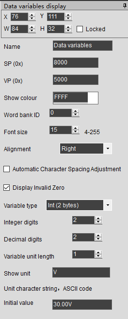
1.6 Data variable display control
(3) OS
//———————————DGUS read and write format
typedef struct
{
u16 addr; //UI 16bit variable address
u8 datLen; //8bitdata length
u8 *pBuf; //8bit data pointer
} UI_packTypeDef; //DGUS read and write packets
//——————————-data variable display control
typedef struct
{
u16 VP;
u16 X;
u16 Y;
u16 Color;
u8 Lib_ID;
u8 FontSize;
u8 Algnment;
u8 IntNum;
u8 DecNum;
u8 Type;
u8 LenUint;
u8 StringUinit[11];
} Number_spTypeDef; //data variable description structure
typedef struct
{
Number_spTypeDef sp; //define SP description pointer
UI_packTypeDef spPack; //define SP variable DGUS read and write package
UI_packTypeDef vpPack; //define vp variable DGUS read and write package
} Number_HandleTypeDef; //data variable structure
With the previous data variable handle definition. Next, define a variable for the voltage sampling display:
Number_HandleTypeDef Hsample;
u16 voltage_sample;
First, execute the initialization function
NumberSP_Init(&Hsample,voltage_sample,0×8000); //0×8000 here is the description pointer
//——Data variable showing SP pointer structure initialization——
void NumberSP_Init(Number_HandleTypeDef *number,u8 *value, u16 numberAddr)
{
number->spPack.addr = numberAddr;
number->spPack.datLen = sizeof(number->sp);
number->spPack.pBuf = (u8 *)&number->sp;
Read_Dgus(&number->spPack);
number->vpPack.addr = number->sp.VP;
switch(number->sp.Type) //The data length of the vp variable is automatically selected according to the data variable type designed in the DGUS interface.
{
case 0:
case 5:
number->vpPack.datLen = 2;
break;
case 1:
case 2:
case 3:
case 6:
number->vpPack.datLen = 4;
case 4:
number->vpPack.datLen = 8;
break;
}
number->vpPack.pBuf = value;
}
After initialization, Hsample.sp is the description pointer of the voltage sampling data variable; Hsample.spPack is the communication pointer between the OS core and the UI voltage sampling data variable through the DGUS interface function; Hsample.vpPack is the attribute of changing the voltage sampling data variable, such as font Colors, etc. are also passed to the UI core through the DGUS interface function. Hsample.vpPack.addr is the voltage sampling data variable address, which has been automatically obtained from the initialization function. When you change the variable address or variable data type in the DGUS interface, there is no need to update the variable address in the OS core synchronously. After the OS core calculates the voltage_sample variable, it only needs to execute the Write_Dgus(&Hsample.vpPack) function to update it. There is no need to pack the voltage_sample for DGUS transmission.
Post time: Jun-15-2022