Specification
Description
Product Tags
ASIC Information
| T5L2 ASIC |
Developed by DWIN. Mass production in 2019,1MBytes Nor Flash on the chip, 512KBytes used to store the user database. |
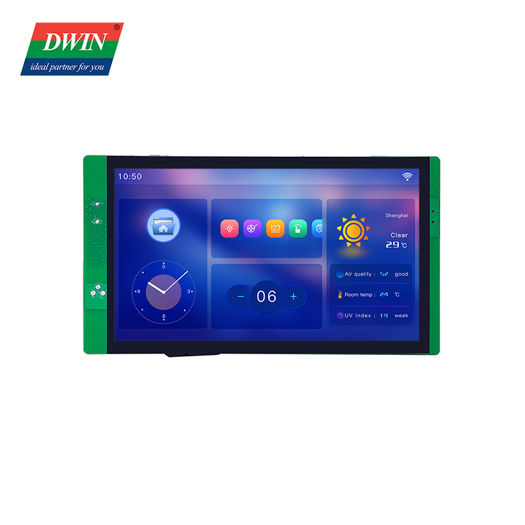
Display
| Color |
16.7M(16777216) colors |
| LCD Type |
IPS TFT LCM ,wide viewing angle |
| Viewing Angle |
Wide viewing angle, 85°/85°/85°/85° (L/R/U/D) |
| Display Area(A.A) |
222.70mm(W)×125.30mm(H) |
| Resolution |
1024×600 Pixel |
| Backlight |
LED |
| Brightness |
EKT101A: 250nit |
Voltage & Current
| Power Voltage |
6v-36v |
| Operation Current |
VCC = +12v, Backlight on,250mA |
| VCC = +12V, Backlight off,110mA |
Reliability Test
| Working Temperature |
-20~70℃ |
| Storage Temperature |
-30~85℃ |
| Working Humidity |
10%~90%RH |
Memory
| Flash |
Space of Font: 4-12Mbytes |
| Picture Storage:12-4Mbytes |
| RAM |
128Kbytes |
| Nor Flash |
512Kbytes |
UI & Peripheral
| UI Version |
TA / DGUSⅡ (DGUSⅡ pre-installed) |
| Peripheral |
Capacitive touch panel, Buzzer |
Dimension
| Dimension |
265.9mm(W) ×148.1mm(H) ×20.7mm(T) |
| Net Weight |
565g |
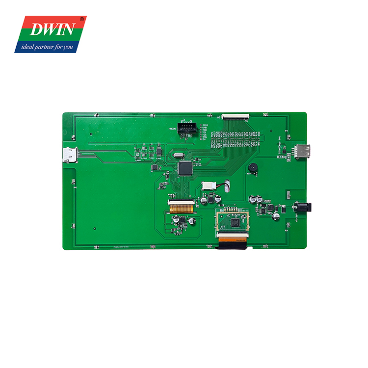
Interface
| Socket |
50Pin-0.5mm FCC |
| USB |
Yes |
| SD Slot |
YES (SDHC/FAT32 Format) |
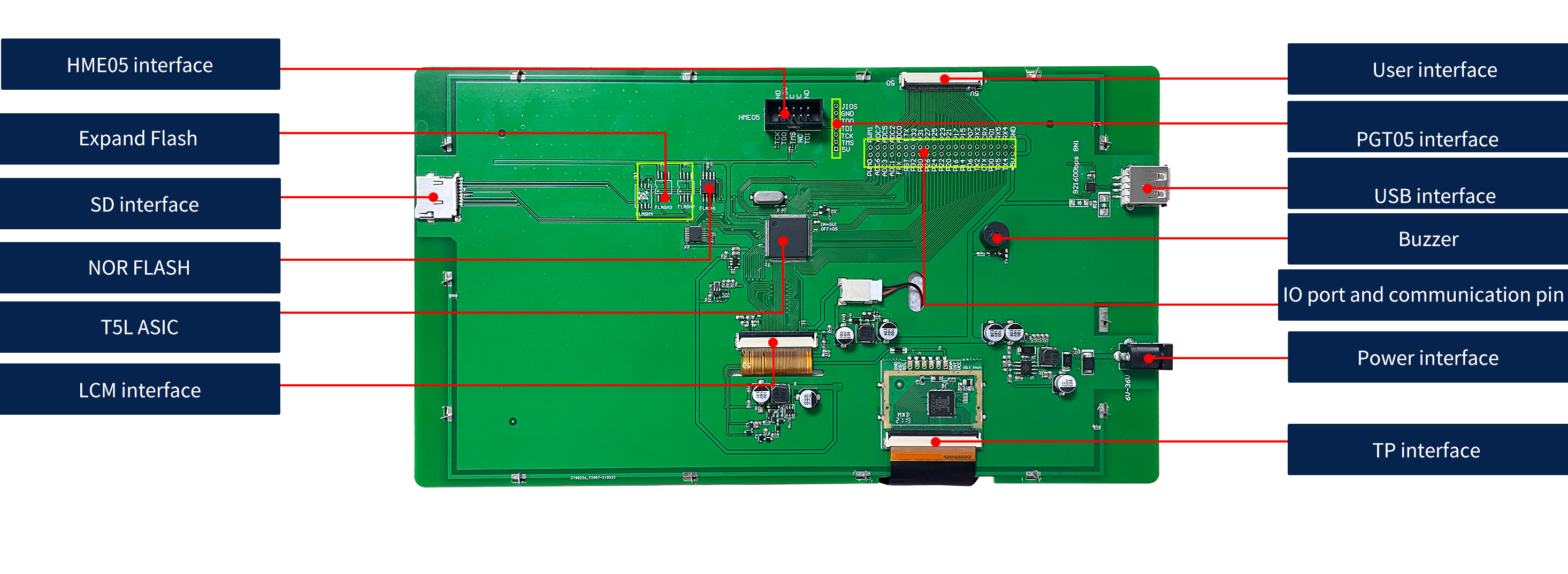
Interface Description
| 1# |
SD card burning interface |
| 2# |
JTAG interface, connect to HME05 emulator, or connect to PGT05 burner to burn the underlying core firmware. |
| 3# |
FLASH expansion module, 3 FLASH modules can be expanded |
| 4# |
2.54mm through-hole pad, GUI/OS CPU lead-out interface, silk screen on the other side |
| 5# |
LCD screen interface |
| 6# |
Capacitive touch screen interface (COB structure) |
| 7# |
USB interface, UART1 can be selected |
| 8# |
6-36V wide voltage power supply interface |
External Interface
| PIN |
Definition |
Description |
| 1# |
GND |
Common ground |
| 2# |
RX4 |
UART4 Data reception |
| 3# |
RX5 |
UART5 Data reception |
| 4# |
P01 |
I / O |
| 5# |
CRX |
CAN interface data reception |
| 6# |
RX2 |
UART2 data receiving |
| 7# |
P07 |
I / O |
| 8# |
P15 |
I / O |
| 9# |
P17 |
I / O |
| 10# |
P21 |
I / O |
| 11# |
P23 |
I / O |
| 12# |
P25 |
I / O |
| 13# |
P27 |
I / O |
| 14# |
P31 |
I / O |
| 15# |
P33 |
I / O |
| 16# |
FTX |
FSK transceiver data reception |
| 17# |
ADC0 |
AD input |
| 18# |
ADC2 |
AD input |
| 19# |
ADC5 |
AD input |
| 20# |
ADC7 |
AD input |
| 21# |
PWM1 |
16bit PWM output |
| 22# |
5V |
power input |
| 23# |
TX4 |
UART4 data transmission |
| 24# |
TX5 |
UART5 data transmission |
| 25# |
P0.0 |
I / O |
| 26# |
CTX |
CAN interface data transmission |
| 27# |
TX2 |
UART2 data transmission |
| 28# |
P06 |
I / O |
| 29# |
P14 |
I / O |
| 30# |
P16 |
I / O |
| 31# |
P20 |
I / O |
| 32# |
P22 |
I / O |
| 33# |
P24 |
I / O |
| 34# |
P26 |
I / O |
| 35# |
P30 |
I / O |
| 36# |
P32 |
I / O |
| 37# |
RSTN |
System reset input |
| 38# |
FRX |
FSK transceiver data transmission |
| 39# |
ADC1 |
AD input |
| 40# |
ADC3 |
AD input |
| 41# |
ADC6 |
AD input |
| 42# |
PWM0 |
16bit PWM output |
Previous: 8.4Inch Evaluation Board
Model:EKT084
Next: T5L ASIC 4 Inch Function Evaluation Board Model: EKT040A